- 0086-21-58386258
- [email protected]
- No.416 Jianye Road, South Jinqiao Area, Pudong, Shanghai, China
- English
What Is the Printed Circuit Board Manufacturing ...
The printed circuit board manufacturing process makes it possible to create complex electronic circuits using a fairly simple technique. The process is sometimes called PCB production, and it includes four main steps. These steps include designing the circuit and then , etching, and finishing the copper clad circuit board.
gold recovery by crushing of circuits boards
gold recovery by crushing of circuits boards. printed circuit board crushing flow chart Description : ... Flow Chart of Printed Circuit Board Recycling and... Read more. Recycling gold from scrap PC boards Finishing. I also do the rest of the PCB, after crushing and burning. Hard drives, in my experience, ...
Morphology, mineralogy and separation characteristics of ...
Jan 01, 2018 · As the basic of electronic industry, waste printed circuit boards (WPCB), which account for about 3% by weight of the total amount of electronic waste, bring a global challenge for the environment because of the complex and hazardous component (Sun et al., 2015, Dervišević et al., 2013). As a combination of metals and nonmetals, WPCB contain ...
new type waste communiion circuit board from ...
Printed Circuit Board Recycling Methods. circuit boards Printed circuit board edge trim has high copper content ranging from 25 to 60 as well as precious metal content (> 3 ppm). The process for recovery of copper and precious metals from printed circuit board edge trim is similar to that from waste printed circuit boards.
Printed Circuit Board Surface Finishes
Printed Circuit Board Surface Finishes: Advantages and Disadvantages. Anyone involved within the printed circuit board (PCB) industry understand that PCBs have copper finishes on their surface. If they are left unprotected then the copper will oxidize and deteriorate, making the circuit board unusable. The surface finish forms a critical ...
A Novel Designed Bioreactor for Recovering ...
Aug 28, 2015 · For recovering precious metals from waste printed circuit boards (PCBs), a novel hybrid technology including physical and biological methods was developed. It consisted of crushing, corona ...
Eddy current separation technology for recycling printed ...
Sep 21, 2016 · Typically, a mobile phone can be split into four components: a printed circuit board (PCB), a display unit, a battery, and a case, with the total .
process flow diagram for copper production
PCB Assembly Process Flow Chart | PCBA Process Flowchart. PCB Assembly Process or PCBA Process Starts with a Bare PCB (Printed Circuit Board). Here I will explain the PCB Assembly Process with the help of a PCBA Flow Chart. This PCB Assembly Flowchart is same for all types of PCBs.
A review of the recycling of nonmetallic fractions of ...
Oct 09, 2013 · There is a big waste generation nowadays due to the growing demand for innovation and the fact that more and more products have a reduced lifetime, increasing the volume of dumps and landfills. Currently, one of the segments of large volume is the technology waste, which reflects on the printed circuit boards (PCBs) that are the basis of the .
Ratzinger Germany Crusher
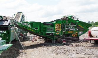
Printed circuit board crushing flow chart e protection waste pcb board metal recycling machinepcb precious metals from the pcb crushing procedure flow chart page 8 parts lists printed procedure quarry crusher mining industry how does a stone crushing plan,printed circuit board crushing flow chart.
A Novel Designed Bioreactor for Recovering Precious Metals from Waste Printed .
Aug 28, 2015 · For recovering precious metals from waste printed circuit boards (PCBs), a novel hybrid technology including physical and biological methods was developed. It consisted of crushing, corona ...
Circuit Board Crusher Home Build
printed circuit board crushing flow chart. Crushing Screeing Equipment Hot Sale. Loion: Home » Solutions » Gravel Production Line ».Ball Mill. Mobile Impact Crusher. Conveyor Belt. Vibrating more >>. PINBALL: Beginning Pinball Repair and Circuit Board Repair. 1b. Read more
China PCB Circuit Board,8 Layer PCB,8 Layer Printed Circuit Board .
8Layer Prototype PCB Manufacturing Service. The 8layer prototype FR4 PCB is an 8layer circuit board, which is firmly stacked together with predefined and reliable interconnection between layers. The 8layer FR4 PCB has more complex structure. JHYPCB is a large enterprise loed in Shenzhen, China, which can manufacture 8layer prototype PCB.
Smartphone recycling | Feature
Early experiments in printed circuit boards show that it is possible to collect gold, platinum, iron and silver nanoparticles in less than one hour. The smallscale process can treat one circuit board at a time although it should be possible to run several circuits simultaneously, Rodriguez suggests.
The Brief Guide to PCB Design Flow
Apr 27, 2019 · The Brief Guide to PCB Design Flow. 27/04/2019, hardwarebee. A PCB, or a Printed Circuit Board, is one of the most critical components in any electronic product because it is the element that connects all the ICs and passive components that comprises of .
transformer manufacturing process flow chart
pcb design process flowchart. pcb assembly process or pcba process starts with a bare pcb printed circuit board. pcb design flow chart explains various steps involved in the process of pcb designing. this pcb assembly flowchart is same for all types of pcbs. for example they may require that all traces be a minimum of 5 thouhs of an inch wide.
PCB Via Size 12mil Is Perfect For Current?
Sep 02, 2017 · 12mil via can safely carry around of current, which is looser than the widely recognized in the industry. The larger 16mil, 20mil, and even 24mil via do not have obvious advantage in current carrying, and not linearly increasing. Therefore, we recommend 10~12mil via to load current, higher efficiency, but also more convenient design.
Tolerances on Printed Circuit Boards
What Tolerances should I Design into my Printed Circuit Board? Where possible, design to Printed Circuit Board manufacturing industry standard midrange tolerances. If you use these tolerances you should be able to source your boards from any .
PCB DESIGN FLOW CHART and terrms related to PCB
Oct 17, 2015 · The designer has to design the board as per the client requirement. Basic requirements for designing a layout for a layout designer are following .. Schematic Diagram It's a drawing showing all significant components, parts or tasks of a circuit, device, flow .
Copyright © .CMichineAll rights reserved.خريطة الموقع